Top
Optoelectronic Devices
Development of
GeSn-based Technologies for Group-IV Optoelectronics
Students: Robert Chen and Colleen Shang
Description: The focus of this project is to develop the Group-IV family of
materials (Si/Ge/Sn) for optoelectronics/photonics applications.
The main target is to achieve a direct or near direct bandgap semiconductor
which can be used to build CMOS compatible laser. This is done by engineering
the bandstructure through the use of strain and compositions of the alloy. For
example, bulk Ge is well-known to be indirect bandgap by 136meV, but the
addition of only ~7% Sn can make the material direct bandgap. This has favorable
properties for many optoelectronic applications.
We are currently investigating both relaxed and strain GeSn-based materials
for device development. Relaxed (Si)GeSn films have been grown using
low-temperature molecular beam epitaxy (MBE) on lattice-matched InGaAs
buffers on GaAs (001). This platform is extremely advantageous in studying
the bulk-like properties of relaxed GeSn films, which are difficult to study
in a lattice-mismatched system due to strain's powerful effect on the
electronic bandstructure. Our work on GeSn films have resulted in the
demonstration of photoluminescence from direct-bandgap GeSn films with up to
8.6% Sn and the demonstration of improved quantum efficiency for light
emission with increasing Sn content.
Such a property has great potential for the development of high-efficiency
photonic devices.
Pseudomorphic GeSn/Ge structures are extremely interesting for development
of light-emitting devices due to predictions of improved quantum efficiency,
carrier confinement, and large net TE gain. Additionally, such structures
can be developed on a Silicon substrate for CMOS integration. We are
investigating the optical and structural properties of these material
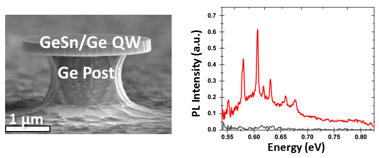
stacks. Using a unique etch-stop feature of GeSn, we are also able to
develop high material quality GeSn/Ge QW microdisk resonators for laser
applications. A process and technology developed here at Stanford has
enabled the creative design of suspended structures with high-quality active
regions. Microdisk resonators with GeSn QWs show strong luminescence and
whispering-gallery-mode resonances in photoluminescence experiments. Such
structures are very interesting for developing on-chip lasers at 2 μm.
We use various characterization techniques to assess the quality of our
films and to understand structural, electrical, and optical changes as a
function of Sn composition and strain. These include XPS, SIMS, AFM, XRD,
SEM, Raman, Photoreflectance, Photoluminescence, and Electroluminescence.
Ge/SiGe Quantum-Well Devices on Silicon for
Optical Interconnects
Students: Ed Fei, Xiaochi Chen, Kai Zang, Ching-Ying Lu, Yijie Huo (research
staff)
Description: There is currently an increasing demand to integrate
optoelectronics with the dominant silicon-based semiconductors for
telecommunications and computer interconnections. Ge has attracted more and more
attentions in recent years due to its pseudo-direct band gap behavior and its
compatibility with Si processing technology. Our research focuses on fabrication
and characterization of high germanium content Ge/SiGe quantum well (QW)
devices, such as modulators, LEDs, lasers and photodetectors, on Si substrate.
The device fabrication involves epitaxial chemical vapor deposition and standard
lithography and is conducted in the Stanford Nanofabrication Facility (SNF). Our
goal is to integrate all these electro-optical interconnections on Si substrate
and realize inter- and intra-chips optical data communication.
Quantum-confined Stark effect (QCSE) in Ge/SiGe quantum wells makes
electro-absorption modulation possible for integrated on-chip optical
interconnects. Prior work established a proof of concept vertical p-i-n QCSE
modulator as well as a vertical PIN resonant cavity device. Future work will
continue to explore metamorphic growth of high Ge content SiGe on Si
substrate using CVD to further research QW properties, including QW material
quality and wavelength tuning. We have also designed and fabricated
horizontal waveguide modulator devices illustrated in the figure 1 for
on-chip optical interconnects.
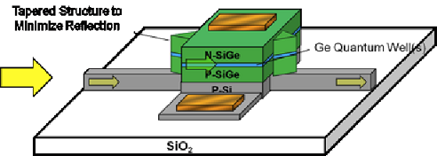
Schematic diagram of a horizontal waveguide modulator device.
Ge/SiGe QW is a potential structure to achieve a low pump power Ge laser for
integrated on-chip optical interconnects. Prior work has shown enhanced
photoluminescence (PL) signal in Ge/SiGe QWs over bulk Ge (below, left) as
well as strong optical resonance in Ge/SiGe QW microdisk structure (below,
right). Future work will focus on material growth, strain engineering and
device fabrication for Ge/SiGe QW microdisk structure lasers.
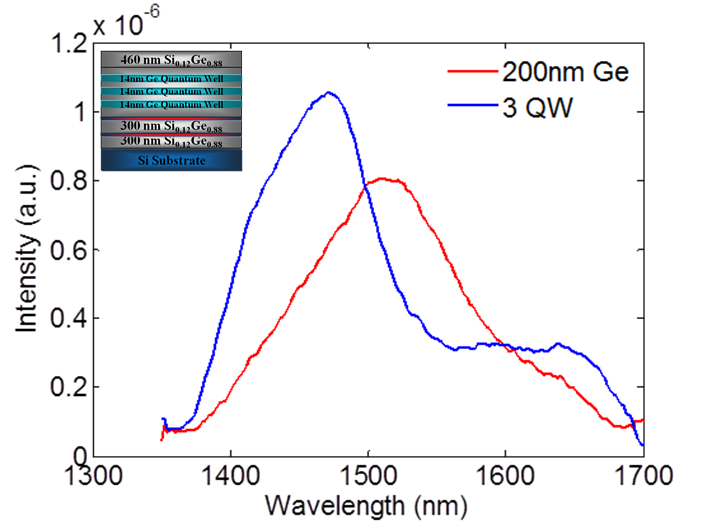

PL signals of bulk Ge and Ge/SiGe QW samples and of
a Ge/SiGe QW microdisk structure.
Long Wavelength GaInNAsSb Vertical Cavity
Lasers
Students: Tomas Sarmiento (post-doc with Prof. Vuckovic)
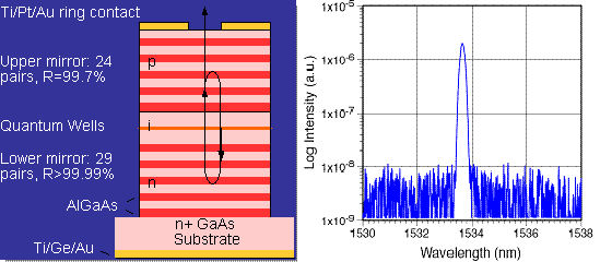
Description: Our work has focused on developing GaInNAsSb on GaAs where we have
realized the lowest threshold current 1.55μm edge-emitting lasers and the first
monolithic 1.55μm VCSELs. GaInNAsSb is a metastable material with many
challenges to realize the longer wavelengths, but the tremendous advantages of
producing long wavelength devices on GaAs where excellent DBR mirror technology
exists and the potential to integrate photonic crystal waveguides and resonators
will enable integration of more functional photonic integrated circuits, arrays
of much lower cost, 2-D lasers and modulators which can be easily coupled into
fiber or utilized in free space architectures and offer great architectural
diversity. Edge emitting lasers from these alloys also offer much greater
opportunity to realize very high power semiconductor laser pumps for Raman
amplifiers and semiconductor optical amplifiers to open up the entire 1.3-1.6μm
low loss fiber region as well as provide resonant pumps for very high power,
high efficiency solid-state lasers. We achieved very low threshold current
density of 373 A/cm2 for 1.55μm edge-emitting lasers and the first GaAs-based
monolithic VCSEL at 1.53μm.
Development of Crystalline Optical Coatings
with Ultra-low Thermal Noise
Students: Angie Lin (post-doc with Prof. Fejer)
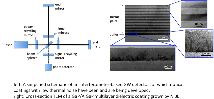
Description: The aim of this project is to
develop crystalline optical coatings from III-V semiconductors such as GaP
and AlGaP that have very low thermal noise, low absorption, and high
reflectivity for applications in precision interferometry such as
gravitational wave (GW) detection and optical atomic clocks. These
instruments rely on having extremely stable Fabry-Perot cavities, however,
one of the dominant noise sources arises from the Brownian thermal noise in
the optical coatings of the cavity's mirrors. Thus, reducing the phase noise
that arises from random motion of atoms in the mirror will improve the
instrument's sensitivity. We have fabricated test mirrors and demonstrated
an order of magnitude reduction in mechanical loss (a measurement directly
related to thermal noise) compared to state-of-the-art optical coatings.
Further understanding of the optical and mechanical loss mechanisms in the
GaP and AlGaP layers will likely lead to continued and systematic
improvements in these new crystalline optical coatings.
A consequence of improving the sensitivity for
the Laser Interferometer Gravitational Wave Observatory (LIGO) is that it
will allow us to greatly expand the volume of the universe from which we can
detect gravitational waves and enable an entirely new field of gravitational
wave astronomy with the worldwide network of detectors. At this exciting
time when several GW detectors around the world are in operation or being
upgraded, humankind is on the brink of directly measuring what Einstein
predicted almost 100 years ago in his theory of general relativity. More
info at: http://ligo.org
Monolithic, Integrated Mode-Locked Lasers
Students: Ken Leedle
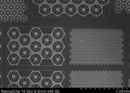
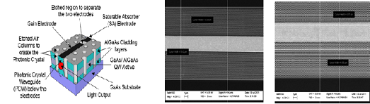
Description: Integrated high power semiconductor mode-locked lasers can be used
for a variety of applications, including compact laser-driven accelerators,
two-photon microscopy, and in-vivo neural imaging in mice. This includes work on
the simulation, design and fabrication of large area Photonic Crystal (PC)
lasers. The devices are simulated using commercial laser simulators PICWave and
CrystalWave by Photon Design Inc. Laser wafers are grown using MBE and MOCVD.
Device fabrication involves standard lithography and also extensive Ebeam
Lithography and is conducted in the Stanford Nanofabrication Facility (SNF).
Laser testing is done is our Harris Optics labs and at the SLAC National
Accelerator Lab. The project combines traditional semiconductor laser design
with nanophotonics.
Sub-picosecond IR laser pulses can be used to scale accelerators 4-5 orders of
magnitude over conventional microwave wavelengths and allow damage thresholds in
the GV/m regime for dielectric materials. Slow light photonic crystal waveguides
will be used to increase the number of cavity modes that mode-lock while keeping
the device itself small, thereby increasing the pulse energy into the mJ range
and decreasing the pulse length to the order of 100fs.
Integrated Index-of-Refraction Bio Sensors
Students: Sage Doshay and Fariah Mahzabeen
Description: This project focuses on the development of miniaturized optical
sensors designed for integrated "lab-on-a-chip" biomedical and bio-defense
applications. Previous work demonstrated a fluorescence sensor with a
monolithically integrated VCSEL, detector, and filter. Current work focuses on
the design, simulation, fabrication, and characterization of an
index-of-refraction sensor using guided resonances in 2D photonic crystal slabs.
Such resonances offer design scalability, light coupling simplicity, and high
sensitivity in a low-loss all-dielectric structure. Fabricated sensors
demonstrate the potential for label-free monitoring of biochemical events such
as virus binding. Ultimately, the fluorescence and index-of-refraction sensors
can be combined on one platform with other detectors to provide portable, rapid,
and correlated bio-analysis.
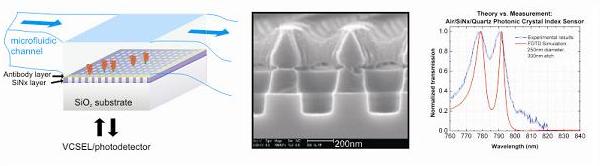
Silicon Nitride photonic crystal slabs were fabricated on quartz substrates
using optical holography. The design targets operation in the near-infrared
transparency window, for low absorption of water and hemoglobin. Initial
measurements agree with 3D Finite Difference Time Domain simulations, and
demonstrate the detection of index changes on the order of 10^-3 for bulk
aqueous solutions. Present work includes the integration of microfluidic
controls and the design/simulation of new sensor architectures for increased
sensitivity. We ultimately aim to combine multiple sensing mechanisms on one
platform to provide rapid, correlated bio-analysis. This is a collaboration with
the Center for High Technology Materials (CHTM) at the University of New Mexico.
In addition, integrated photonic systems are under research for in-vivo
biosensors analyzing whole blood coagulation processes. The integrated system
consists of fiber-based input terminals and photonic crystal platform by which
the allocation and transmission of optical signals are processes. The fabricated
biosensor performs the real-time analysis on whole blood coagulation as a
function of the amount of thromboplastin. It is the fundamental principle that
the time-varying amount of the coagulation catalyst results in time-dependent
refractive index of the whole blood which is monitored by the input signals from
fibers. This enables controlling the coagulation processes by real-time
medication eventually. The research is accomplished by fusing photonics,
nanofabrication, and electrical engineering in the collaboration with the
medical school as well.